Edge Emitting Diode
Edge-Emitting Diode (EED), more commonly known as an Edge-Emitting Laser Diode (EEL) or Edge-Emitting LED, is a semiconductor optoelectronic device where light generation and emission occur primarily from the edge (cleaved facet) of the chip, with the optical mode propagating parallel (in-plane) to the wafer surface.
This contrasts with surface-emitting devices like VCSELs (Vertical-Cavity Surface-Emitting Lasers), which emit perpendicular to the wafer.
Basic Structure and Technical Principles:
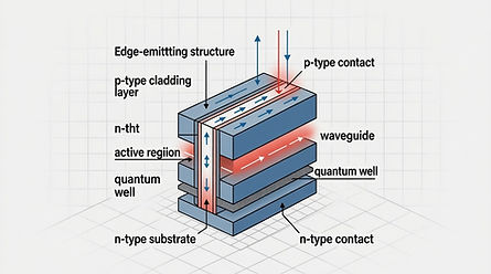
An edge-emitting diode is built on a semiconductor wafer (typically III-V compounds like GaAs, InP, GaN, or AlGaAs). Key layers include:
Active Region: Where electron-hole recombination occurs. Modern designs use quantum wells (QW), multiple quantum wells (MQW), or quantum dots for enhanced carrier confinement, higher gain, lower threshold current, and better temperature stability.
Cladding Layers: Higher-bandgap material surrounding the active region to form a double heterostructure (DH). This provides both carrier confinement (electrons/holes) and optical confinement via refractive index differences, creating a waveguide.
Waveguide: Guides the light along the plane of the chip. The resonator is typically a Fabry-Perot cavity formed by cleaving the crystal to create parallel facets (mirrors via Fresnel reflection, ~30% reflectivity for uncoated GaAs/air interfaces).
Contacts: p- and n-type for electrical injection. Stripe geometry (ridge or buried heterostructure) confines current laterally for single-mode or controlled multi-mode operation.
Operating Principle:
Forward bias injects carriers into the active region.
Spontaneous emission occurs initially (LED mode).
At threshold current, stimulated emission dominates: photons stimulate further recombination, producing coherent light.
Light amplifies along the waveguide, reflects between facets, and a portion exits the front facet (often with anti-reflection coating) while the rear facet may have high-reflection coating.
Key Technical Parameters:
Wavelengths: 650–980 nm (GaAs-based), 1310/1550 nm (InP-based for telecom), visible (red/green/blue for displays), or mid-IR.
Output Power: From mW (low-power) to tens of watts (high-power bars/arrays).
Beam Characteristics: Highly divergent and elliptical (fast axis ~30–40° perpendicular to junction, slow axis ~10° parallel) due to the small waveguide aperture. Requires optics (lenses, fibers) for collimation/coupling.
Threshold Current: Can be as low as a few mA in optimized quantum-well designs.
Efficiency: Wall-plug efficiency often 30–60%+; high gain from longer cavity lengths (hundreds of µm to several mm).
Modes: Can support single longitudinal/transverse mode (e.g., DFB or DBR variants with gratings) or multi-mode.
Photonics Aspects:
Strong waveguide integration compatibility with photonic integrated circuits (PICs). Light propagates in-plane, enabling efficient butt-coupling or hybrid integration with silicon photonics, waveguides, or other components.
Coatings: Critical anti-reflection (AR) on output facet and high-reflection (HR) on rear for maximizing power and minimizing losses. Thin-film deposition is key in manufacturing.
Thermal Management: Junction heating affects wavelength (shifts ~0.3 nm/°C) and efficiency; requires heatsinking, especially in high-power devices.
Laser Applications in Photonics:
Edge-emitting diodes excel in high-power, high-coherence scenarios where VCSELs may fall short:
Telecommunications & Data Centers: Primary light sources for long-haul and metro fiber-optic links (DFB-EELs at 1310/1550 nm). High power and good coupling efficiency into single-mode fibers support high data rates.
Optical Pumping: Pump solid-state lasers (e.g., 808/980 nm for Nd:YAG or fiber lasers) and erbium-doped fiber amplifiers (EDFAs).
Industrial Processing: Material cutting, welding, marking, and additive manufacturing. High-power diode laser bars/arrays deliver kW-level output when stacked.
Sensing & LiDAR: Used in automotive/industrial LiDAR for 3D mapping due to high peak power in pulsed operation and narrow linewidth. Also in spectroscopy and gas sensing.
Medical & Biomedical: Dermatology, surgery, photodynamic therapy, and optical coherence tomography (OCT).
Consumer/AR/VR & Displays: RGB EELs for high-brightness projectors or augmented reality waveguides, offering efficiency advantages at certain power levels.
Optical Storage & Printing: Historically in CD/DVD/Blu-ray; still in laser printers.
Military/Defense: Directed energy, range finding, and countermeasures.
Advantages over Surface Emitters:
Higher output power and brightness.
Better beam quality in the slow axis.
Longer cavities → higher single-pass gain.
Mature manufacturing for high-power applications.
Challenges:
Elliptical/divergent beam requiring correction optics.
Lower on-wafer testability (facets exposed only after dicing).
Thermal rollover and catastrophic optical damage (COD) at high powers.
Polarization and astigmatism management.
Edge-emitting diodes remain foundational in photonics due to their power scalability, wavelength flexibility, and integration potential. Ongoing advances in quantum-dot active regions, coupled waveguides, and heterogeneous integration (e.g., with silicon photonics) continue to expand their capabilities.
Edge-emitting LEDs (non-lasing variants) exist for applications needing broader spectrum and lower coherence (e.g., some illumination or low-cost fiber links), but laser versions dominate high-performance uses.